Please feel free to add/edit this page as you come across cool things in Eagle!
Getting the Software
- Eagle is installed on all of the computers in the GM lab. If you want a personal copy, the freeware version is available for download here. You'll also find lots of user-defined libraries that may contain parts that you're looking for.
Starting a new project
- File > New > Project, give it a name
- File > New > Schematic, save, give it a name
- File > Switch to board, choose yes
Accessing Libraries
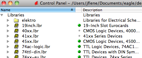
For some reason, libraries (even the default ones) are not set up in the "use" mode, meaning that components from those libraries can't be placed in a schematic. To turn on an individual library, click the little circle next to the library in the control panel, turning it into a green dot:
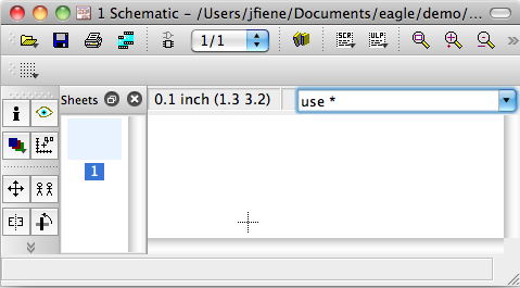
To turn on all of the libraries at once, execute the "use *" command in the schematic window:
Searching for Parts
Though it sure would be nice, there doesn't seem to be a way to search through the libraries in the control panel. It seems the best way to find what you're looking for is by trying to add the part to a schematic. Once you click the "Add a part" button:

You will see a browser and a search box. The search functionality is limited, and the best hint is to encapsulate anything you're looking for in asterisks (which serve as wildcards), like this:
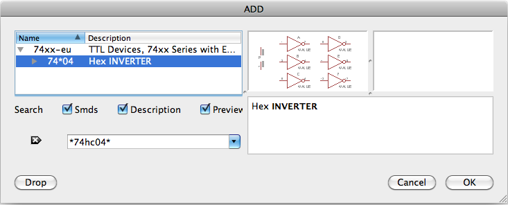
Performing this same search without the asterisks returns zero results, which is very frustrating!
And DO NOT CLICK THE DROP BUTTON! If you do, it will temporarily disable certain library elements. To get them back, run the "use *" script described in the "Accessing Libraries" section above.
Dealing with multi-gate ICs
- For many logic chips that have multiple gates in a single IC (the 74HC06 hex inverter, for instance), you need to be careful about how you handle power and ground. If you happen to use the standard VCC and GND, Eagle will automagically connect the supply lines for the logic chip. If, however, you need to use a different source, or if you want to be explicit, click the Invoke button:

The click on one of the logic gates, which will bring up something like the following:
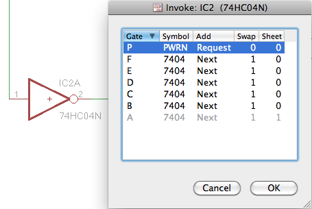
Select the line that says something about power (here it's PWRN), and click OK. Now you should be able to place the power and ground pins in your schematic, like this:
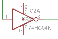
To add a second gate from the same package, once again use the Invoke tool, but this time select one of the other gates (shown as B-F in the image above).
Other Schematic-Capture Hints
- Power and ground can be found in the 'supply1' library - the standard are VCC and GND.
- Resistors, capacitors, and inductors can be found under 'resistor'
- To move more than one thing at a time, use the group tool to select around them, double click to finish selecting, then right click on one of the members of the group, and select "move: group"
- ALWAYS double check the dimensions and pinouts of components against your actual parts!
Board Layout Hints
- To change layers when routing a trace (add a via), switch the layer, and it will put a via at the switch point once you're done routing - don't forget to set the via shape first
- To add a ground field or plane, select the polygon tool, set the isolate value, then draw a shape (make sure it closes - this is often easier with coarse grid spacing), which will show up as a dashed line. Now, click the name button, double click on one of the dashed lines, and change the name to match your ground net (GND, most likely). Now, click the ratsnets button to have it generate the filled region.
- To add vias (outside of trace laying), place it, then use the name tool to change it's name to whatever you're trying to connect it to
- To put soldermask over vias, select Tools > DRC, then on the mask tab, set the limit to larger than your drill (or perhaps it's pad OD?) size, and it will mask over them - this is mostly useful for keeping your silkscreen clean.
- To move the label without moving the part, or to change the font size, select "Edit > Smash", then click on the component
- ALWAYS double check the dimensions and pinouts of components against your actual parts!
Gerber file output
- File > Cam Processor -or- Film strip icon
- File > Open > Job... > excellon.cam
- Process Job
- File > Open > Job... > gerber274x.cam
turn off mirror for Solder Side and Solder Stop Mask SOL
you may want to turn off tPlace layer in Silk screen CMP tab - Process Job
- go look at your files, which you may see:
.cmp = component side metal
.drd = drill data, location of the drill holes
.dri = a text file for you, do not send to the boardhouse
.gpi = a text file for you, do not send to the boardhouse
.plc = silkscreen for component side
.sol = solder side metal
.stc = mask stop for component side
.sts = mask stop for solder side - to check your gerber output
www.freedfm.comgerbv
- to generate an x,y,theta list of components, run mountsmd.ulp
Tutorials