MEAM.Design - S62 - Preparing an Eagle Board File for the S62
<< | S62 | Generating Gerber Files for S62 >>
Trace & Space:
- Please make sure that trace width and signal spacing is a minimum of 0.008 in (2 mm) wide and that polygons have an isolation value of at least 0.012 in. The smallest mill we currently have is 0.2 mm, and even hitting this width can be tricky, so plan your board accordingly.
Board Area:
- We have 6" x 6" and 11" x 8" boards stocked, however a little bit of margin space should be utilized for fiducial markers and test cuts that are made during the milling process.
Board thickness:
- The substrate for our boards is 0.063" thick FR-4. Our 6" x 6" boards have two sides of 1 oz/ft2 copper, but 11" x 8" boards are available in both 1 oz/ft2 and 2 oz/ft2 thicknesses.
- 4 oz/ft2 is NOT available. Plan your trace widths for high current applications accordingly.
Drills:
- For drilling holes, see the chart of available drill sizes below.
- Please make sure your holes are close to these sizes. Failing to adhere to the available drill sizes will cause ill-sized or even missing annular rings around vias and through-holes.
- The only exception to the above rule is with holes equal to or larger than 3.0 mm. For these over-sized holes, CircuitCAM will automatically have the S62 use a routing bit to cut the hole.
List of Available Drill Sizes
| Drill Size (In) | Drill Size(mm) |
| 0.019 | .5 |
| 0.024 | .6 |
| 0.028 | .7 |
| 0.031 | .8 |
| 0.035 | .9 |
| 0.039 | 1.0 |
| 0.047 | 1.2 |
| 0.059 | 1.5 |
| 0.061 | 1.55 |
| 0.116 | 2.95 |
| 0.118 | 3.0 |
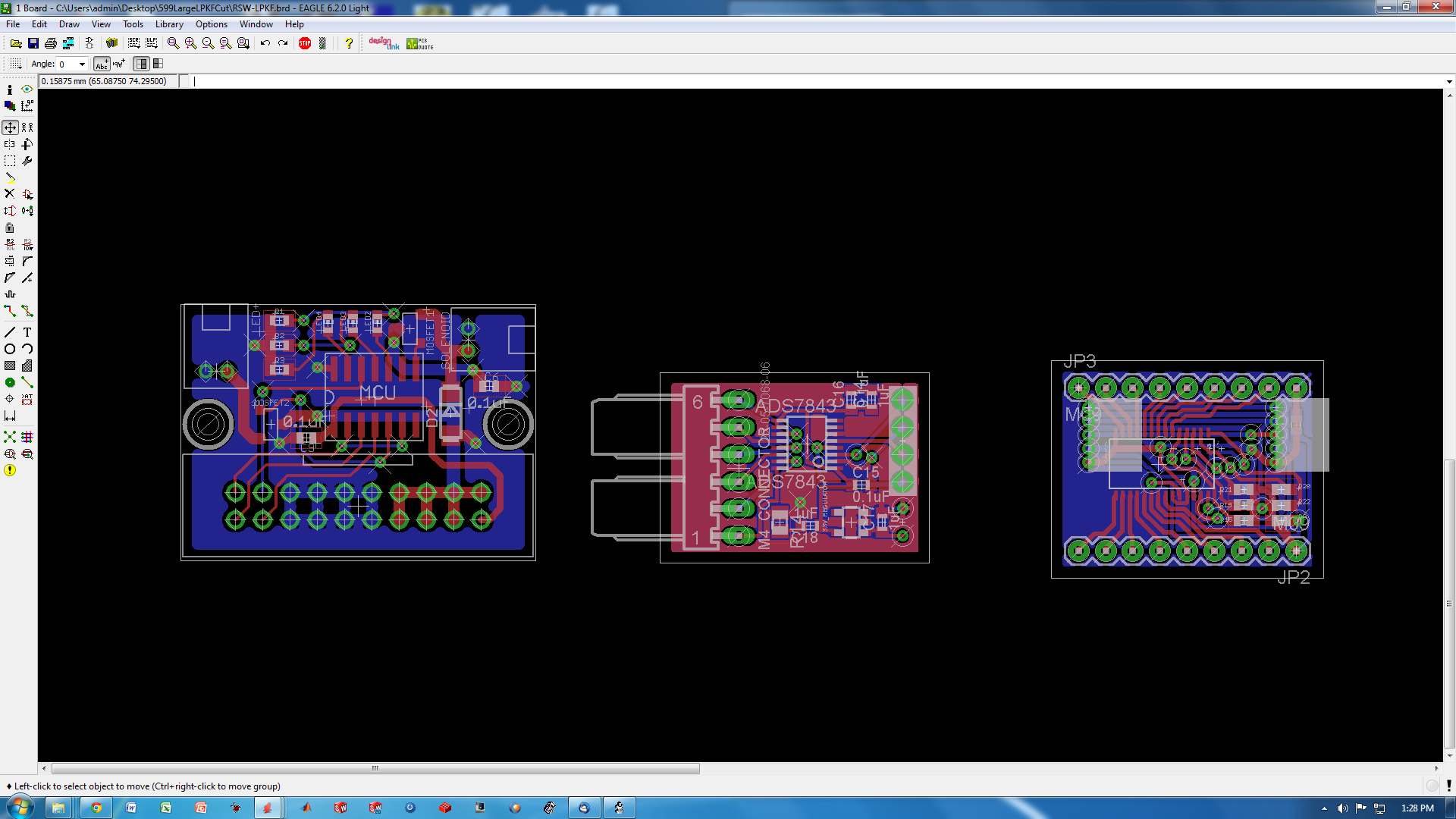
Cutting a single board:
- If cutting a single board, you may then use the CAM processor to generate the necessary Gerber files for the S62
Cutting multiple boards:
- Create and save a new .brd file in a new location and do not take any steps to generate a new schematic.
- One at a time, copy the individual boards you would like to make from their respective .brd files and paste them to the new .brd file. If you wish to make multiples of the same board, simply paste as many times as necessary.
- Make sure that all boards are at least 0.237in (0.6 mm) away from each other to leave enough space for the S62 to cut out the boards with it's routing bits.
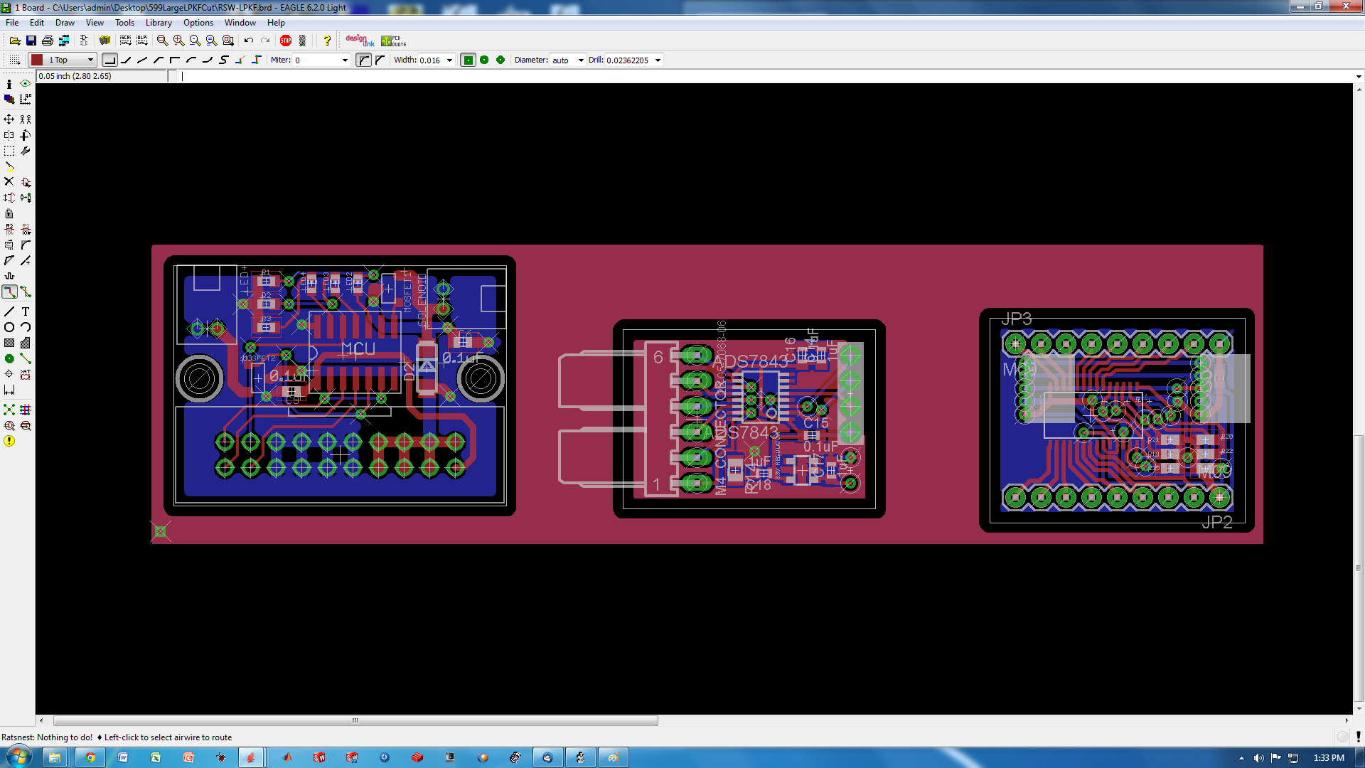
- Place a polygon across all boards in the layout on both the top and bottom layer.
- Name the polygons you just created with the same signal name and make sure they do not share a signal name with any signal on the boards. As shown below, this provides a solid copper region between the boards. This solid region of copper will not be milled by the S62 and thus will save time in the process. These polygons will not fill in space inside the boards.