MEAM.Design - S62 - Generating Tool Paths From Gerber Files
<< Generating Gerber Files for S62 | S62 | Using Board Master >>
Once the Gerber files have been saved, you can use CircuitCAM to make an LMD file. This LMD file is needed in later steps, where you will import it into Board Master (yet another software), and begin to drill & cut your board.
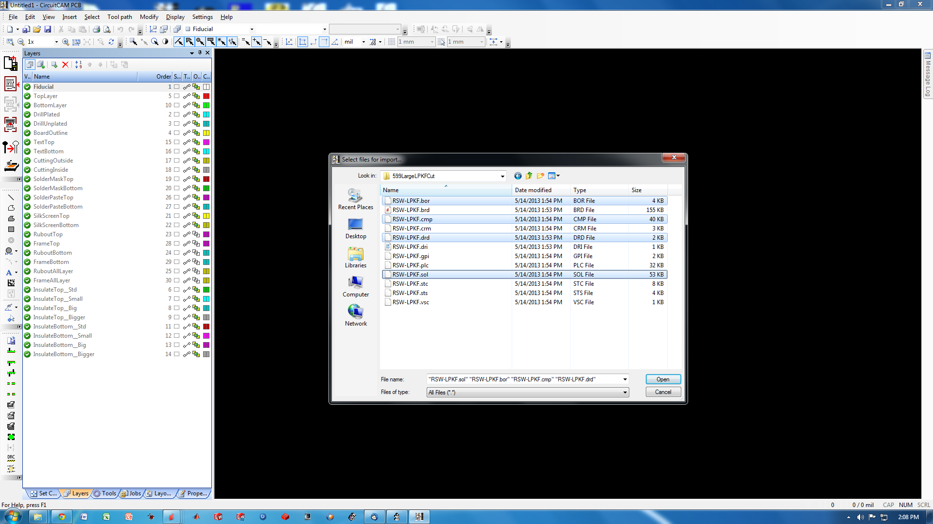
In CircuitCAM, click [File -> Import] and select the .drd, .bor, .sol, and .cmp files.
Click 'OK'.
Next, assign each of the imported files to a layer. There should be one layer for each of the Gerber files (four layers in total). CircuitCAM will use these four layers to produce the LMD file. Assign the files like this:
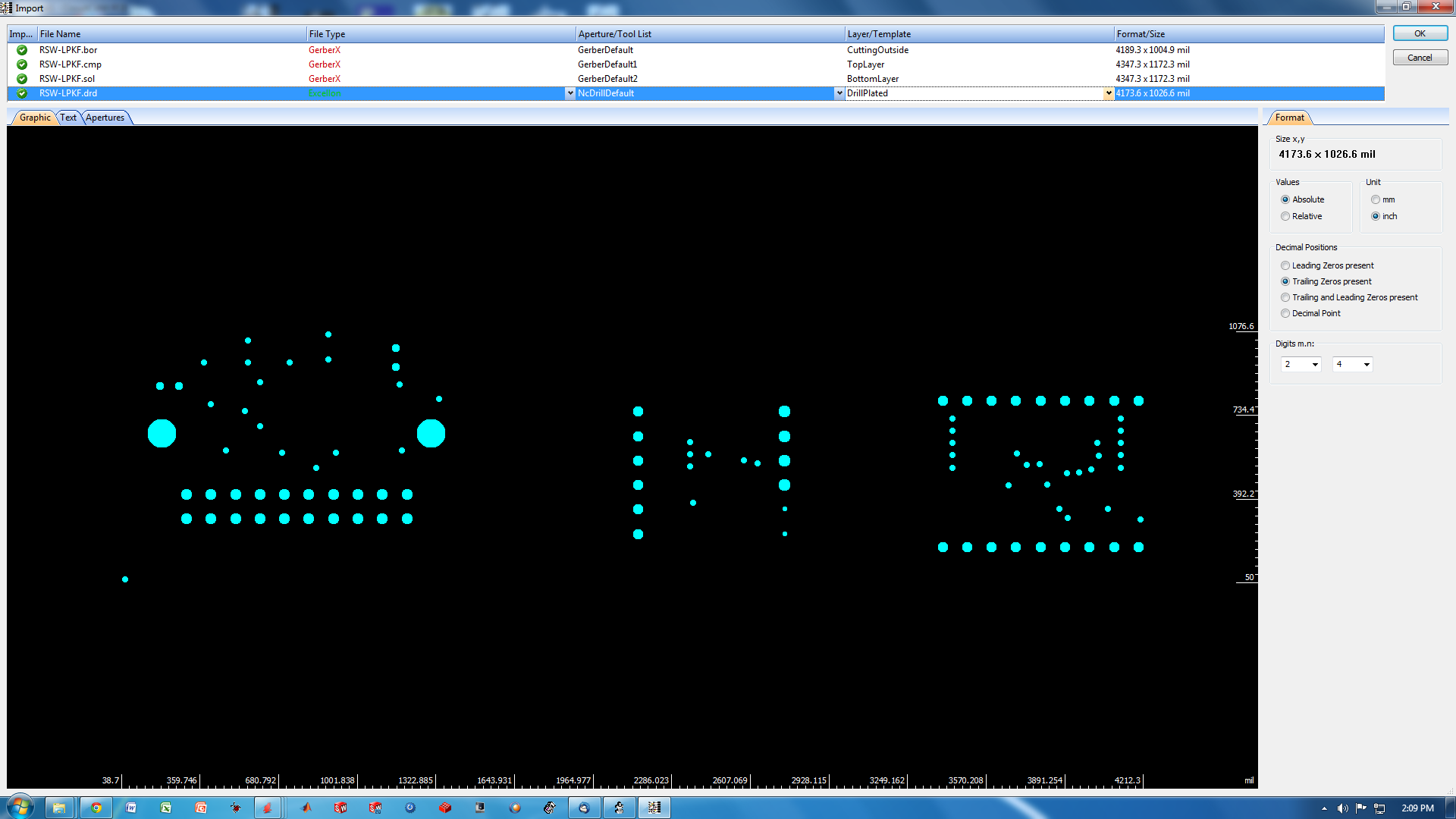
Click 'OK'.
Now you will see something like this:

First you have to tell CircuitCAM what part of the blank copper sheet you want to use as your working area. This is called the 'Rubout Area'.
Click on the 'RuboutAllLayer' item in the list on the left hand column, and hit the ENTER key. It should become bold, indicating that it has been successfully selected.
Use the rectangle or polygon tool to enclose the board(s), leaving some space around the outside, for the release-cutting step, which comes later.

Now, select the positions for the Fiducial holes. Select the 'Fiducials' item in the list on the left hand column, and hit the ENTER key. It should become bold, indicating that it has been successfully selected.
Click on the circle tool. The diameter must be as shown in the image below in order for the camera to be able to detect them properly.
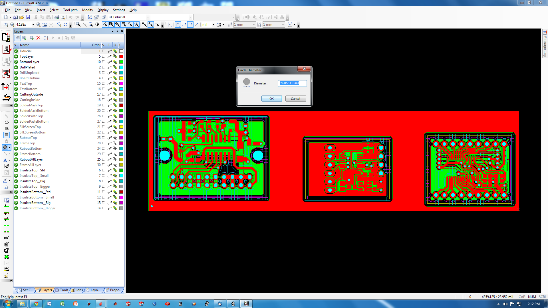
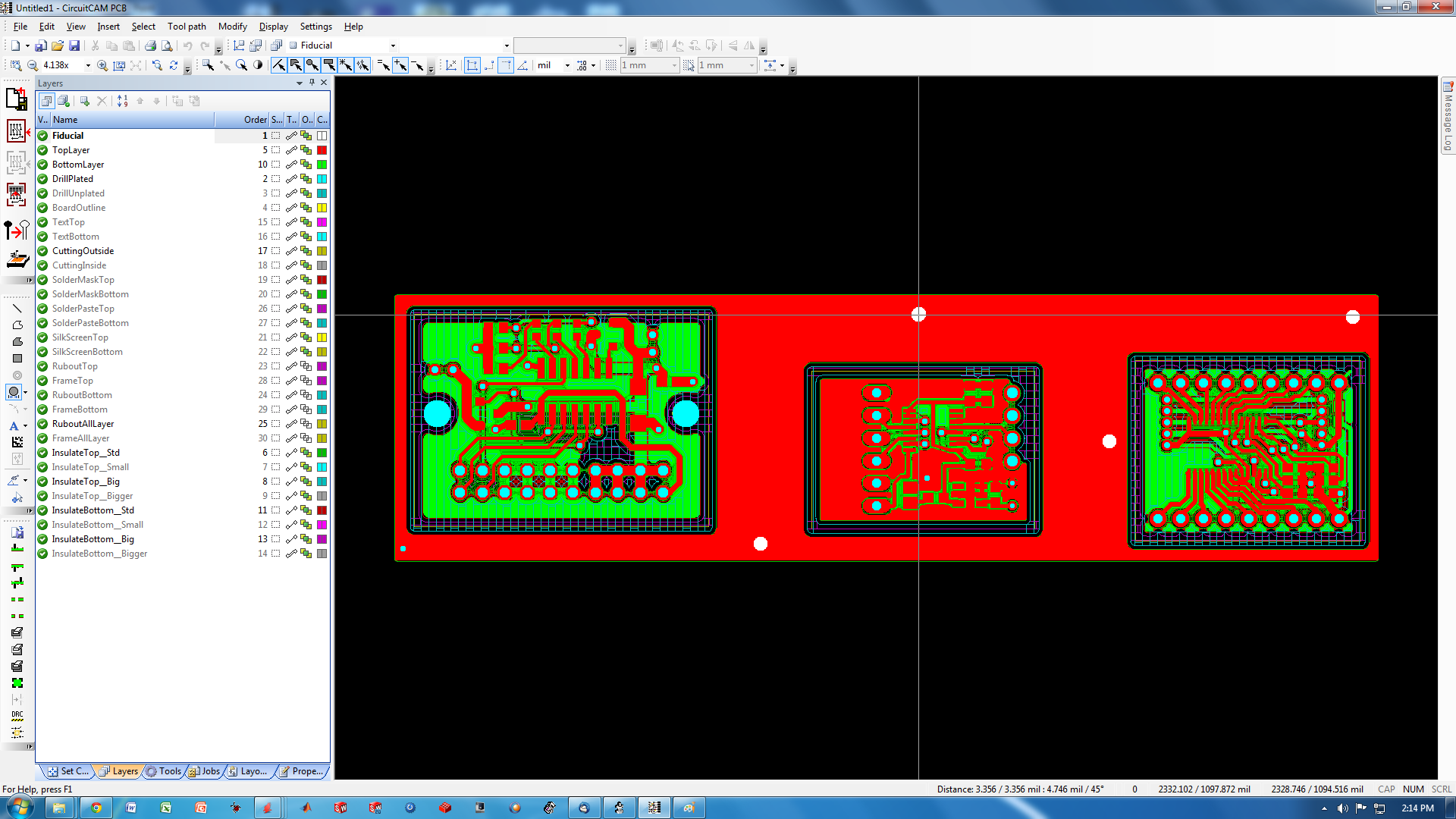
Now place four holes. The relative positions of the holes will affect how accurately the Board Master software (which uses the camera on the S62) is able to determine the board position and orientation.
To improve accuracy, aim for a good spread in both the x and y directions, as pictured below.
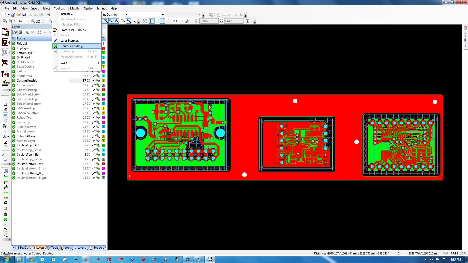
Next we have to tell CircuitCAM which cutting profile to use when releasing the boards from the copper sheet at the end of the manufacturing process.
This is known as the 'Cutting Outside' process, and is done using a tool called a contour router. The image below shows how to navigate to the Contour Routing menu.
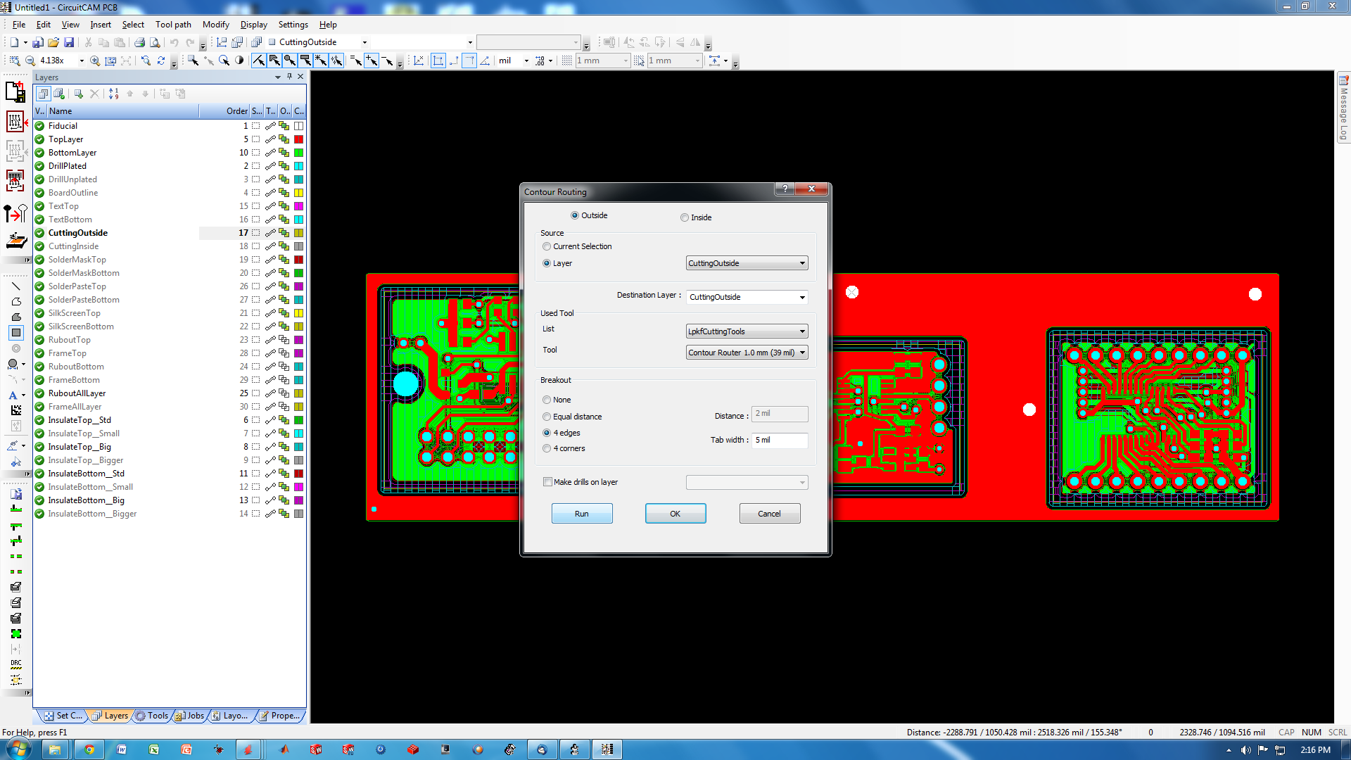
The Contour Routing menu is shown in the image below. Adjust the settings so they appear as pictured. You may change from a 1.0mm contour router to a 2.0mm one if preferred.
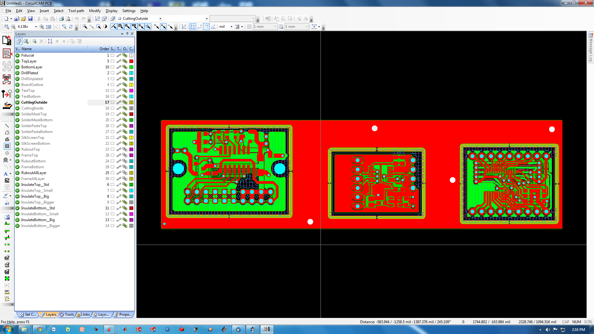
Click 'Run'. Your board(s) should now look like the image below, with a thick yellow line around the perimeter of each one. This shows the tool path that will be used in the 'Cutting Outside' step.
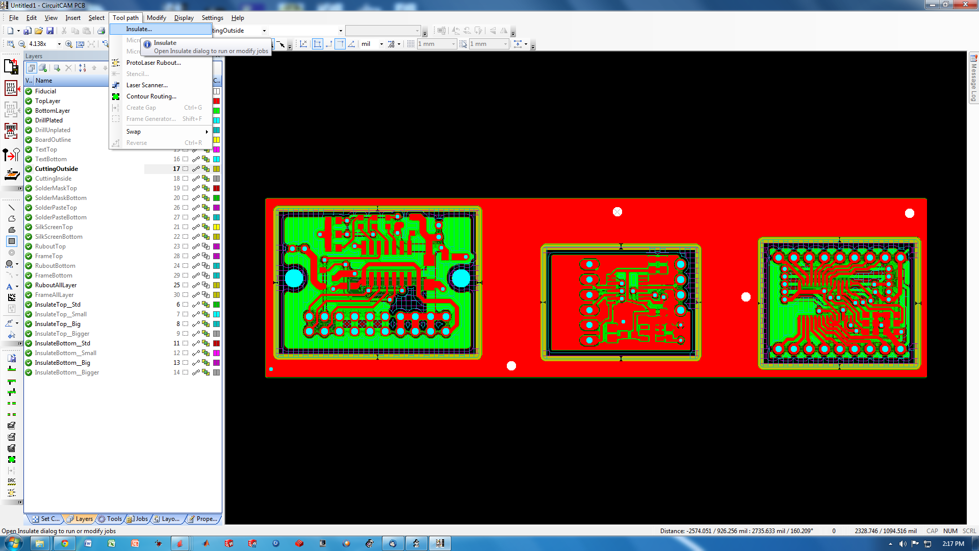
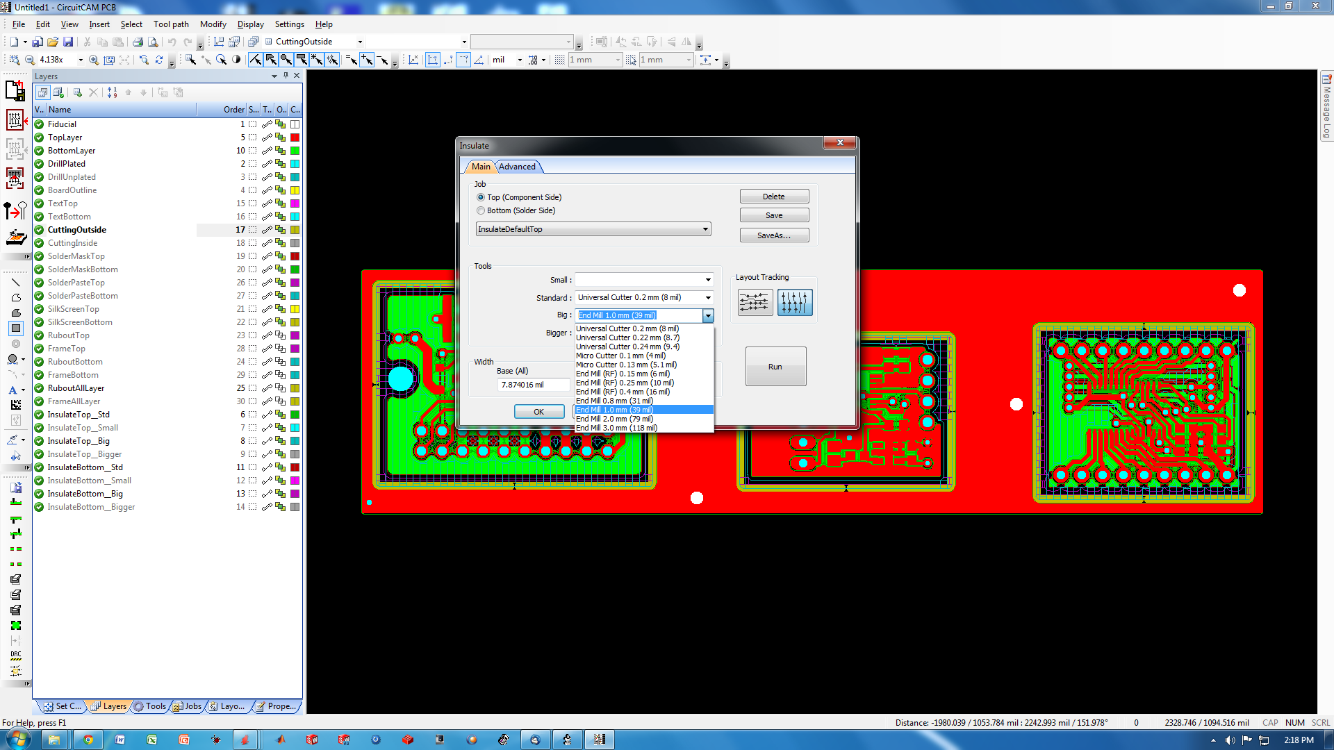
CircuitCAM lets you pick what sizes of tools are used in the milling steps. Milling (also called 'Insulating') is usually done in two steps: large features and small features.
Picking larger or smaller tools can affect how much time it will take to complete your board(s).
In the Insulate menu, you can use the pulldown menu to select tools from the list. Make sure you actually have the tools that your choose! Note that the top and bottom sides of the board can be configured independently of one another.
When you are finished, click the 'Run' button.
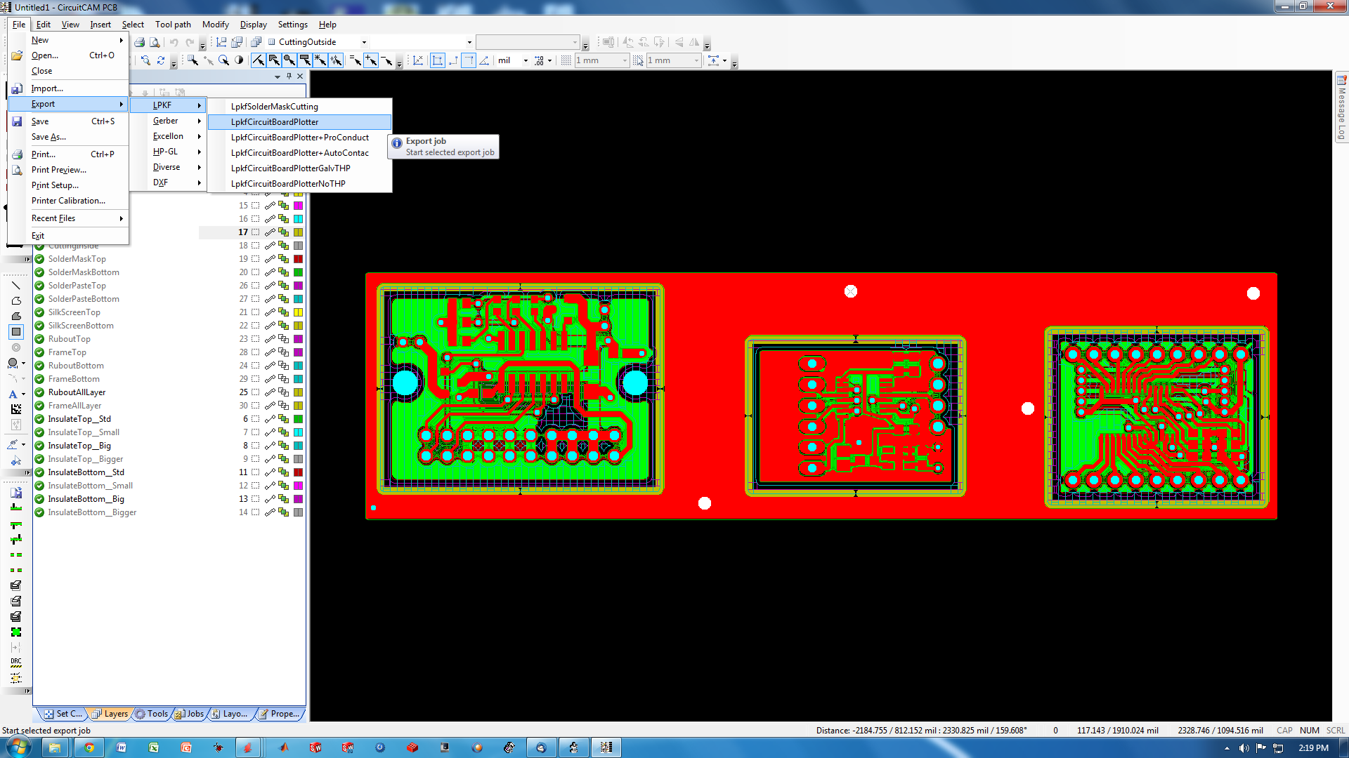
Now click the 'Insulate All Layers' button as shown below. When you do this, CircuitCAM generates the tool paths that will be used by the S62.

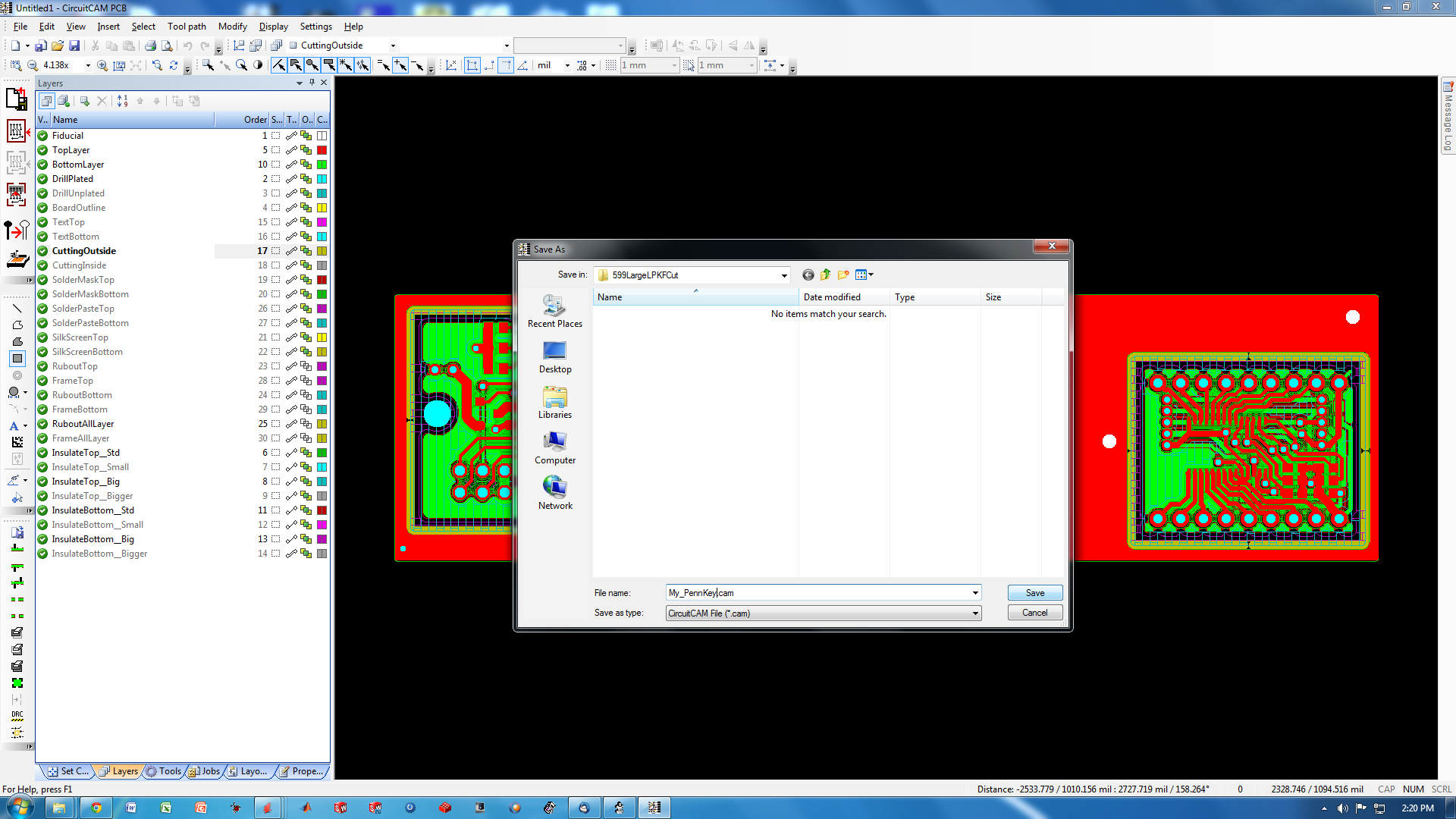
Click 'Export', and save the .LMD file in the same directory as the Gerber files, using a distinctive filename (such as your PennKey) so you can easily distinguish it from the rest of the files in the next step.
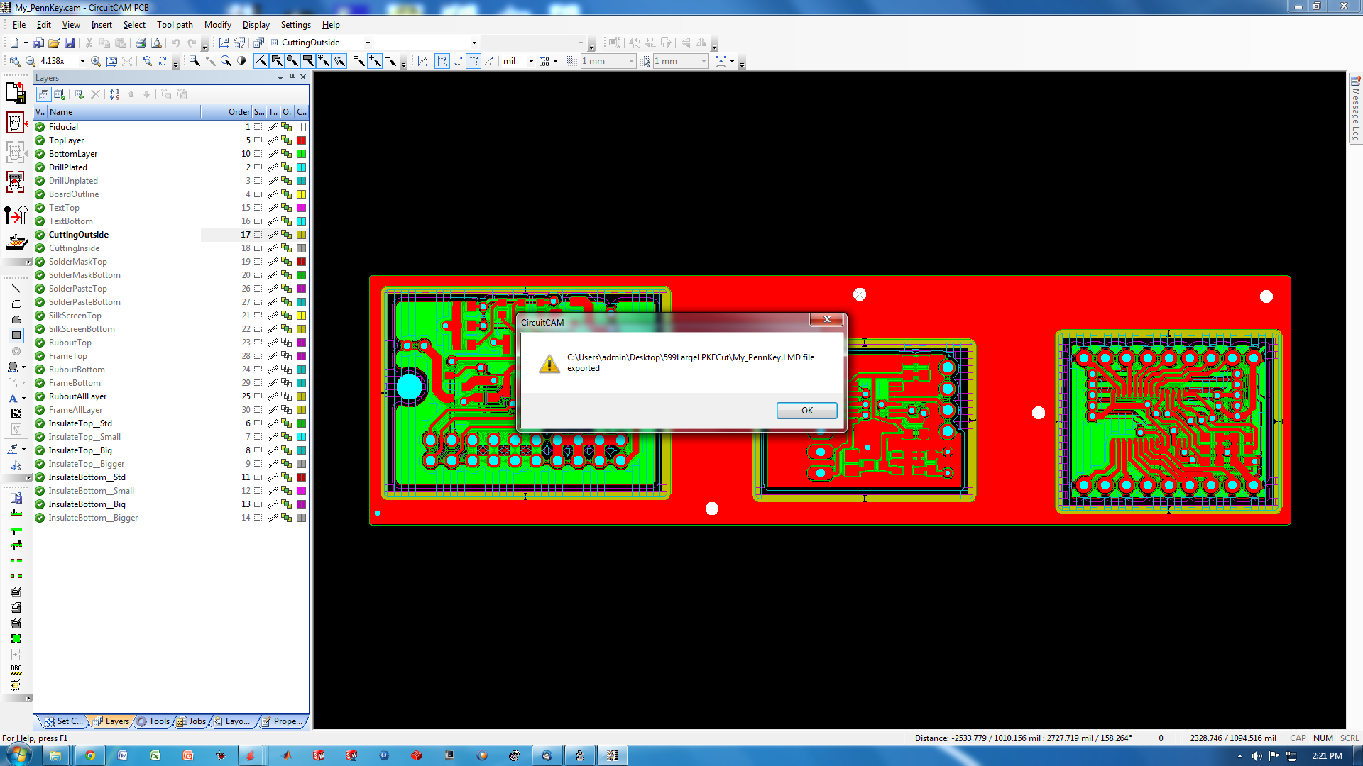
Once the file has been exported, you will see a dialog appear, as shown in the image below. It appears to be an error message, but this is simply indicating that the .LMD file was successfully exported.
You're done. You can now close the CircuitCAM software.